breaking down Etched's Sohu
what the patents, first principles, and math actually tell us (speculative)

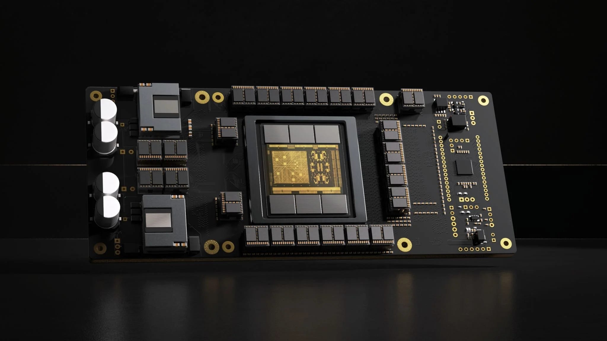
Etched has raised $625 million to build a chip that can only run transformers. they claim 20x faster than an H100 for transformer inference. the chip hasn’t shipped. no independent benchmarks exist. but peter thiel says he sold his entire nvidia position after investing.
i will break down what could be real, what’s still undefined but could be real, and speculate on what design decisions Etched has (maybe) made. i will run through the math of the chip from the patents, math, and first principles.
a lot of this will be speculative, using reasoning, first principles, and my opinion on what could make sense to do with the information i could find.
most coverage of Etched falls into two camps: revolutionary or vaporware. neither is useful if you actually want to understand what they’re building and whether the physics supports the claims. so i went through their three published patents, ran the memory math, and read every primary source i could find.
here’s my breakdown of what i think is actually going on.
the problem Etched is solving (from first principles)
to understand why someone would build a transformer-only chip, you need to understand what happens inside a transformer forward pass and why GPUs are bad at it.
a transformer layer does two things: attention and feed-forward (FF). attention figures out which tokens in the sequence are relevant to each other. FF processes the result through two large matrix multiplications with a nonlinear activation in between. then you repeat this 80 times for a model like llama 70B.
if you need a refresher on this, you should watch 3blue1brown:
both attention and FF are dominated by matrix multiplications, which is what systolic arrays (the tensor cores inside Nvidia GPUs) are built for. so GPUs should be great at this. and they are very good at this for both training and inference. but for inference, the story is more complicated (and interesting).
during inference, especially autoregressive decode (where the model generates one token at a time), the batch of work per step can be very small. a single decode step for a single request involves multiplying one vector against enormous weight matrices. the systolic array, which is designed to multiply large matrices against each other, barely has anything to do. most of the time is spent waiting for memory to deliver the weights.
nvidia reports the H100 achieves about 30-40% utilization of its tensor cores during typical inference workloads. that means 60-70% of the most expensive silicon on the chip is sitting idle.
where GPU transistors actually go
etched’s marketing says “only 3.3% of H100 transistors are for matrix multiplication.” this number gets repeated everywhere and it deserves a bit of scrutiny.
the math behind it: the H100 has 528 tensor cores, each with 512 FMA (fused multiply-add) circuits. each FP16 FMA requires roughly 10,000 transistors. so 528 x 512 x 10,000 = ~2.7 billion transistors out of 80 billion total. that’s 3.3%.
the arithmetic is correct. but the framing is (a bit) misleading.
the implicit claim is that 96.7% of the chip is wasted overhead from programmability, and that an ASIC could reclaim all of it.
but let’s look at where those transistors actually go:
the H100’s L2 cache is about 60MB. at TSMC 4nm SRAM densities, that’s roughly 17 billion transistors just for the cache bit cells, so around 20-25% of the chip. the L1/shared memory across all 144 SMs adds another 36MB, about 10-12 billion transistors. the register files add another 36MB on top of that.
add in the HBM memory controllers (12 channels, 512-bit each), the NVLink SerDes, PCIe interfaces, and you’ve accounted for maybe 70-80% of the chip in things that any chip doing large-scale matrix multiplication needs. you need caches to stage data. you need register files to hold operands. you need memory controllers to feed the HBM. an ASIC needs all of this too.
the stuff an ASIC can actually eliminate is warp schedulers, instruction fetch/decode units, general-purpose dispatch logic, RT cores, MIG partitioning. this is maybe 10-15% of the die. not 96.7%.
so in my opinion, the honest version of Etched’s argument should be: we can reclaim 10-15% of die area by removing programmability overhead, and reinvest it in more compute. that gives us maybe 2-3x more raw compute density.
where does the rest of etched’s claimed 20x advantage come from? utilization. if you can get 90% utilization instead of 30-40%, that’s a 2.5-3x multiplier on top of the 2-3x from silicon reallocation. and if your architecture lets attention and FF run in parallel instead of sequentially, that’s another significant factor.
combined, these get you into the range of plausible 10-20x, but my take here is that the mechanism is heavily relying on utilization and parallel execution, not the transistor reallocation story from the marketing.
the dual-engine architecture (from the patents)
etched has three published patent applications. the first and most revealing is US20240419516A1, “Parallel execution of self-attention-based AI models,” filed June 2023.
the patent describes an IC with two distinct compute blocks running in parallel:
a systolic array handles operations that don’t depend on data from previous tokens: QKV projections, the output projection, the feed-forward network, and layer normalization. these are all large, regular matrix multiplications where the systolic array excels.
a self-attention circuit handles operations that do depend on previous tokens, the Q x K^T score computation, softmax, and value aggregation. these operations have different compute characteristics: smaller matrices, irregular access patterns for the KV cache, and a nonlinear operation (softmax) interleaved with the matrix multiplications.
critically, each engine has its own dedicated HBM memory. the systolic array’s HBM stores weights (which flow top-down through the array). the self-attention circuit’s HBM stores the KV cache. this means weight reads and KV cache reads never contend for the same memory bandwidth. on a GPU, both workloads fight over the same HBM channels.
the patent is describing a chip where the memory hierarchy is co-designed with the compute, so that the two fundamentally different workloads in a transformer — FF and attention — each get their own dedicated path from memory to compute.
if you’ve read bjarke roune’s writing on AI chip design (this is a truly excellent book, and i cannot recommend it enough. read it here), this should look familiar. he describes the problem of “mono-sized systolic arrays” — where the same compute unit handles both attention (small K dimension, memory-intensive) and FF (large K dimension, compute-intensive), and is always underutilized for one or the other. his proposed solution: “have one FF core with a huge systolic array, to be used for FF, and also having several smaller attention cores, each with a smaller systolic array, to be used for attention. all on the same chip.”
etched appears to have built exactly that, except they went further by hardwiring the entire transformer graph rather than keeping it programmable.
why the dual-engine design could actually make sense
there’s a recent paper from EPFL (Lin et al., 2025, “SystolicAttention”) that quantifies exactly why existing hardware fails at attention.
on AWS NeuronCore-v2, the matmul throughput is 90 TFLOPs/s. the vector unit throughput (for softmax and other non-linear operations) is 2.3 TFLOPs/s. this is roughly a ~40x gap.
FlashAttention needs to frequently interleave matrix multiplications with softmax computations. on a standard systolic-array accelerator, every time you need to do softmax, you have to stop the systolic array, offload to the vector unit, wait for the much slower vector unit to finish, and then restart the systolic array. the systolic array sits idle during every softmax step.
the EPFL group’s solution (Fused Systolic Array) gets 1.77x higher attention utilization than NeuronCore-v2 and 4.83x higher than TPUv5e by running FlashAttention entirely within a modified systolic array.
etched’s solution is even more radical: build a completely separate circuit for attention that doesn’t have this bottleneck. the self-attention circuit handles the interleaved matmul-softmax-matmul pattern natively, while the systolic array focuses exclusively on the large, regular matrix multiplications where it excels.
the patent describes the self-attention circuit as “not limited to any particular type of circuit” — it could be a smaller systolic array, a microprocessor, a controller, or an ALU.
scaling to multiple chips
the second patent (US20240378175A1, “Multi-Chip Systolic Arrays,” filed may 2023) describes how to scale beyond a single die.
the key idea is that all ICs are identical, so you tile them in a grid. horizontal connections between chips are bidirectional (activations flow both ways). vertical connections are unidirectional (weights flow top-down only). this is a weight-stationary dataflow, weights get loaded once and stay in place while activations stream through.
memory chips are hardwired to specific columns of the systolic array without any switching element. this eliminates the overhead of a memory interconnect but means the memory mapping is fixed at manufacturing time.
a row of 4 chips with 100x100 local systolic arrays forms one 100x400 combined array. the patent claims this can scale to arrays of 100-10,000 rows by 100-10,000 columns of dot product units.
the compiler
the third patent (US20250138820A1, “Model-Specific ASIC Compilation Using Fused Kernel Replacement”) covers the compiler. it recognizes “specialized functions” in PyTorch/TensorFlow code, fused operations like “layer normalization followed by linear transformation”, and translates them to an intermediate representation for the ASIC. the same model code can compile for GPU (for training) or for Sohu (for inference).
this is a much simpler compiler problem than CUDA or XLA. you only need to handle the handful of fused operations that transformers use, not arbitrary compute graphs.
stress-testing the claims with math
etched claims 500,000+ tokens per second on llama 70B with an 8-chip server (FP8, 2048 input tokens, 128 output tokens, 8-way model parallelism). let’s check if this is physically possible.
the first constraint is memory. an 8-chip server has 1,152 GB total (144GB per chip x 8). llama 70B in FP8 requires about 70GB for weights, or ~140GB when you account for the overhead of model parallelism buffers and activation memory. call it 140GB for weights, leaving ~1,012 GB for KV cache.
for llama 70B with GQA, the KV cache is:
per token per layer: 8 kv_heads x 128 head_dim x 2 (K+V) x 1 byte (FP8) = 2 KB
per token all layers: 2 KB x 80 = 160 KB
at batch size 1000 with 2048-token context (matching their benchmark):
KV cache = 1000 x 2048 x 160 KB = 320 GB
that fits. 140 GB weights + 320 GB KV cache = 460 GB, leaving 692 GB of headroom.
but push the context to 4096 tokens:
KV cache = 1000 x 4096 x 160 KB = 640 GB
total = 780 GB — still fits, but less comfortably.
at 8192 tokens:
KV cache = 1000 x 8192 x 160 KB = 1,280 GB
total = 1,420 GB — does not fit in 1,152 GB.
if using BF16 KV cache (2 bytes per element instead of 1), everything gets worse by 2x. batch-1000 at 4K context in BF16 = 1,420 GB. doesn’t fit.
the benchmark conditions (2048 input / 128 output) are not an accident. real production workloads serving chatgpt-style requests with 8K+ context at high batch sizes would either need aggressive KV cache quantization or much smaller batches, which kills the throughput advantage.
the second constraint is memory bandwidth. Sohu has roughly 4,800 GB/s of HBM bandwidth (estimated from the HBM3E configuration). the H100 has 3,350 GB/s. only about a 1.4x difference.
for autoregressive decode at low batch sizes, inference is memory-bandwidth-bound: you’re reading the entire weight matrix for each token. at batch-1, the maximum throughput is limited by how fast you can stream weights from HBM, and Sohu’s 1.4x bandwidth advantage would give roughly 1.4x throughput.
the 20x only works at very high batch sizes, where the same weights are reused across many requests. in this regime, inference becomes compute-bound, and Sohu higher utilization (90% vs 30-40%) and dedicated dual-engine architecture pay off. the math roughly works: ~3x from silicon reallocation and higher peak compute x ~3x from utilization x ~2x from parallel attention/FF execution = ~18x. this is close to the actual 20x, which is believable given how little public information is available and how much of the math is just from estimating here.
Sohu is a throughput machine, not a latency machine. this is the opposite of SRAM-based chips like Groq or d-Matrix, they optimized for single-digit-batch latency.
Etched goes the other direction: massive batch throughput using HBM.
the bitcoin ASIC analogy
etched invokes the bitcoin mining ASIC analogy constantly. gavin: “whether or not you’re a fan of cryptocurrency, the bitcoin mining ASIC companies have been able to do quite well for themselves.”
the analogy is actually useful.
here’s what happened with bitcoin: mining went from CPU (2009) to GPU (2010) to FPGA (2011) to ASIC (january 2013, when canaan shipped the avalon 1). GPU mining became obsolete overnight. the first ASICs were ~13x faster than GPUs. over the next decade, bitcoin ASICs achieved a 497x improvement in energy efficiency. bitmain captured 75-82% of the market. SHA-256 ASICs are one of the most successful specialization stories in computing history.
the analogy works directionally. there is a real economic force toward specialization when a workload is important enough and stable enough. AI inference is clearly important enough.
i believe this argument is correct, but there’s a small structural difference that could limit how far the analogy could carry.
SHA-256 is immutable. it hasn’t changed since 2001. it will never change. every transistor on a bitcoin ASIC can be dedicated to one fixed computation for the lifetime of the chip.
transformer architectures change every 6-12 months. new routing (MoE, expert choice), new attention mechanisms (multi-query, grouped-query, sliding window, linear attention), new activations (SwiGLU, GeGLU), new normalization schemes (RMSNorm, DeepNorm), new precision formats (FP8, FP4, MXFP4).
bitcoin ASICs achieved 100,000x efficiency over GPUs. transformer ASICs could theoretically cap at maybe 10-50x, because you can’t strip away everything when the target keeps moving.
a fun fact here is that Etched’s chief architect, saptadeep pal, co-founded auradine before joining etched. auradine is a bitcoin mining ASIC company making 3nm chips at TSMC.
the transformer bet
etched’s entire existence hinges on one question: will transformers remain the dominant architecture for AI inference?
the bull case is strong. GPT-2 and llama-3 are architecturally very similar despite being 5 years apart. the differences are scale and minor tweaks (SwiGLU, RoPE, GQA). transformers survived the CNN era, the RNN era, and multiple “transformer killer” challenges.
petros lamb articulated the most sophisticated version of this argument in what he calls the “transformer attractor” thesis. the idea: transformers and GPU silicon have co-evolved into a stable equilibrium. any alternative architecture faces a two-gate trap: it must simultaneously clear hardware compatibility (can it saturate tensor cores?) AND institutional backing (will a major lab bet on it?). the gates reinforce each other: poor hardware compatibility makes institutional bets unattractive, which means no one writes optimized kernels, which keeps hardware compatibility poor.
mamba is the canonical example. it started with elegant linear-time parallel scans. by mamba-2, the authors rewrote the core to use matrix multiplications because scans can’t saturate tensor cores. the paper explicitly states this. the architecture changed to fit the hardware.
what I actually think
the dual-engine architecture is a real and defensible technical idea. the dedicated HBM split for weights vs KV cache is clever hardware-software co-design. the multi-chip scaling approach is elegant.
the 20x throughput claim is plausible at high batch sizes with short context. i believe it is not plausible at low batch sizes or long context, but that’s ok. the benchmark conditions (2048 input, 128 output) are chosen to maximize the advantage. real production workloads will see less.
the team is the strongest signal that makes me excited about Etched.
the obvious frequently stated risk is that transformers are not the dominant architecture, but another big risk is not that transformers go away. it’s that they evolve into something sohu can’t run as well, so they don’t get a massive advantage over NVIDIA. e.g. hybrid attention-SSM architectures.
if the chip ships and the benchmarks hold at production scale, etched will have built one of the most consequential pieces of silicon in AI history.
Excellent post as always! Please update the link to Bjarke Hammersholt Roune's book to: https://docs.google.com/document/d/1dZ3vF8GE8_gx6tl52sOaUVEPq0ybmai1xvu3uk89_is/edit?usp=sharing